Our Technology
Our work over the last ten years has allowed us to solve the many challenges faced by thermoelectric power generators, opening up a wide range of potential applications in industry and beyond.
Disrupting the industry
We believe that the primary market opportunity in the thermoelectric space is the breakthrough development of a high performance material that can be manufactured using low cost bulk methods. A commercial device must target efficiencies of 15% plus, and a production cost of $1 per watt to unlock the rapid growth potential in various markets. None of the spectacular gains in thermoelectric performance regularly reported at universities or research institutes have been transferred into the marketplace, largely because they are based upon approaches that are too intricate and expensive for the commercial world.
The reason why MicroPower’s technology is such an important breakthrough is that it can deliver high efficiency at low cost, and in a temperature range of 300°C – 1000°C and beyond that opens up opportunities not served by the current materials.
Can we say with 100% certainty that no other company can make the same claim? No, but what we can say is that all of our current partners and customers (including two US Government labs, both experts in the field) tell us that no-one else has delivered prototype devices that come close to matching MicroPower’s products in terms of performance, durability and commercial viability.
Below is an explanation of how we have developed this competitive edge in an increasingly popular marketplace.
What do we make and how does it work?
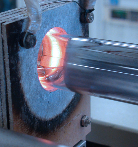
World class base material
Our base material has always needed to possess different qualities to standard thermoelectric material for it to be suitable for our patented barrier layer (see below). Combining mechanical stability, barrier compatibility and solid starting power output required extensive testing and analysis in conjunction with a world leader in this field.
During this process we realised that that is was indeed possible to obtain the characteristics we required, and significantly enhance the energy density of the base semiconductor material.
We then brought this expertise and equipment in-house, providing us with a world class base material production capability on-site which allows us to continue to improve performance and begin to explore alternative materials.
Barrier layer enhancements
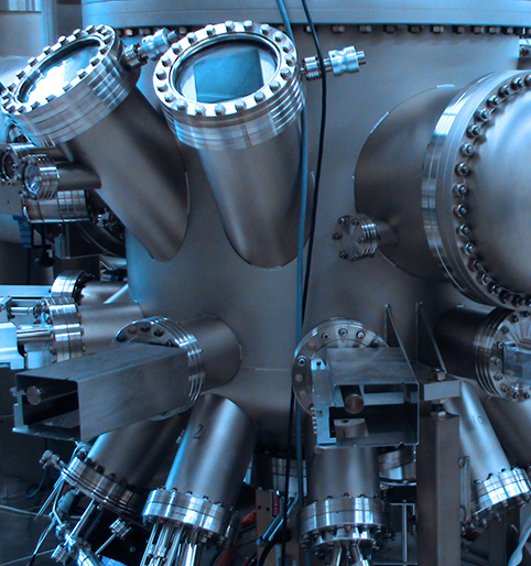
A key factor in our ability to produce highly efficient chips is what we call the “barrier layer”. By depositing atoms in certain concentrations and in certain geometries, we can significantly enhance the efficiency of any semiconductor material that exhibits an easy change of conductivity through doping.
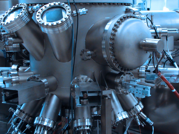
To do this, we use a molecular beam epitaxy tool which, once considered too expensive for commercial production, can carry this out cost-effectively. In addition, the ability to augment the performance of alternative thermoelectric materials mitigates the risk of operating in only two material systems.
Another future area of development that has already been proven in the lab is the ability to "stack" two or more barrier layers on the material, ramping up efficiency even further.
High temperature interconnects
Applying metal plates to chips to enable them to be electrically connected in a module, without losing efficiency, sounds like a straightforward engineering task. However, while this issue has been, to a large extent, overcome in BiTe modules (<250°C), it soon became clear to us that there was no such solution for higher temperature operation.
Consequently, we entered into an R&D agreement with the US Army Research Lab to develop mechanically stable, high temperature compatible interconnect structures for our material, and novel plating techniques were subsequently developed to apply these metal structures to our chips.
Subsequent module making experience with the contact structures precipitated the need to further enhance the ARL hot contact formulation and novel plating techniques were developed to apply the contact metal structures to the PbTe and TAGS chips.
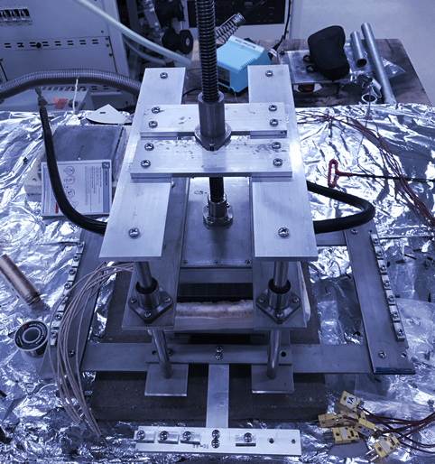
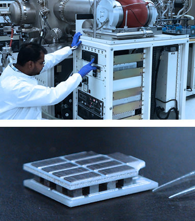
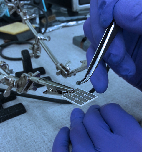
Module and sub-system expertise
From MicroPower’s beginnings, the plan had always been to produce chips and outsource module manufacturing to an existing firm. However, to put it simply, no-one knew how to make commercial high-temperature modules because it had never been done before. Consequently, while there has been some minor support from outside, MicroPower has effectively had to develop this module production capability itself. While the obvious drawback has been the time it has taken, we now have our own bespoke module manufacturing capability which provides us with greater knowledge and control moving forward.
In addition, engineering consulting agreements have been established as a separate revenue stream. There are active agreements with several companies targeted towards integration of MicroPower modules and arrays into specific products. MicroPower has also produced module characterization tools already delivered to several customers, facilitating confidence.